
Keywords: AVR, GPIO, Atmega32
Every micro-controller has GPIO ports. GPIO stands for general purpose input output. These GPIO ports are used to take input on a micro-controller pin or output a value on micro-controller pin.
We will learn how to use AVR ports and program them to read or write from port pins. Now the port has multiple pins associated with it. For example Atmega32 has 8-bit port, i.e. it has 8 pins in a single port. Each bit represents a pin i.e. bit 0 represents pin 0 on that port and so on. As you can see in the diagram given below, Atmega32 has 4 ports named as A, B, C & D. Each of these ports has 8-pins (micro-controller pins).
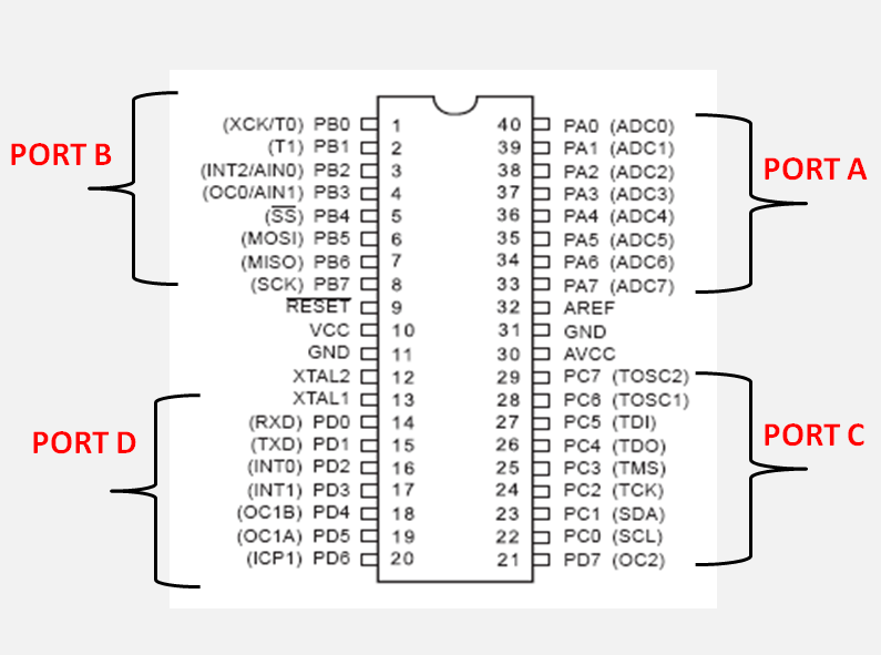
Note that these port pins might have multiple functionality i.e. you can use them as GPIO or as UART or ADC etc. You can use a port pin for a single functionality at a time. You don’t need to worry about this right now; I’ll cover this in a later tutorial.
GPIO REGISTERS
Every GPIO has three registers associated with it in order to control a particular pin. For AVR micro-controllers these registers are:
DDRn – Data Direction Register
PORTn – Port Output data Register
PINn – Port Input Register
n- Indicates the port name i.e. A, B, C & D
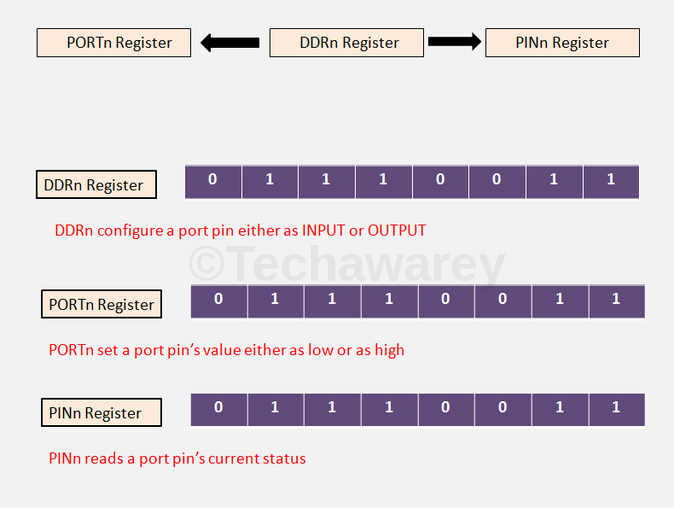
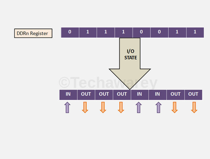
DDRn Register- Data Direction Register configures data direction of a port or a port pin. I mean a port will used for input or output.
Writing a value 0 configure that port pin as INPUT and writing a value 1 configures a port pin as OUTPUT.
Let’s assume we want to configure Port D as OUTPUT:
DDRD = 0xFF; //HEX NOTATION
Or DDRD = 0b11111111; //BINARY NOTATION
Now if we want to configure port D as INPUT:
DDRD =0x00;
Note that it’s not necessary to configure a whole port as input or output. You can configure a single pin as input or output as well.
Suppose you want to configure only 2nd bit (pin) as OUTPUT:
DDRD |= 0x02;
Please read “Register Bit Manipulation” article. Here I have explained Boolean mathematics concept that is being used in bit-manipulation.
PORTn Register- PORTn register is used for two purposes :
(1) To output data when port is configured as output
(2) To activate/deactivate internal pull-up registers when port is configures as input
1. To output data – When configured as output, PORTn register controls the HIGH/LOW state of a port pin. Writing value 1 places that port pin in HIGH state and writing a value 0 places that port in LOW state.

Let’s assume that we want to set port D’s pins in high state, then first we have to configure port D as output using DDRD register and then we’ll place it in high state using PORTD register.
DDRD =0xFF; //Configure Port D as OUPUT
PORTD=0xFF;//Place Port D in High state
2. To activate/deactivate internal pull-up register – When you set bits in DDRn to 0, i.e. make port pins as inputs, then corresponding bits in PORTn register are used to activate/deactivate pull-up registers associated with that pin. In order to activate pull-up resister, set bit in PORTn to 1, and to deactivate (i.e to make port pin tri stated) set it to 0.
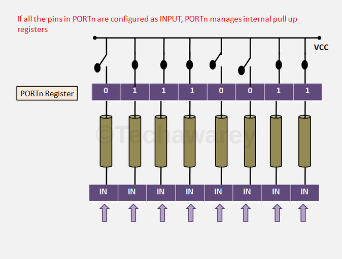
In input mode, when pull-up is enabled, default state of pin becomes ’1′. So even if you don’t connect anything to pin and if you try to read it, it will read as 1. Now, when you externally drive that pin to zero(i.e. connect to ground / or pull-down), only then it will be read as 0.
However, if you configure pin as tri state. Then pin goes into state of high impedance. We can say, it is now simply connected to input of some OpAmp inside the micro-controller and no other circuit is driving it from micro-controller. Thus pin has very high impedance. In this case, if pin is left floating (i.e. kept unconnected) then even small static charge present on surrounding objects can change logic state of pin. If you try to read corresponding bit in pin register, its state cannot be predicted. This may cause your program to go haywire, if it depends on input from that particular pin.
Thus while, taking inputs from pins / using micro-switches to take input, always enable pull-up resistors on input pins.
NOTE: while using on chip ADC, ADC port pins must be configured as tri stated input. I’ll cover it later in ADC example.
Let’s you want to activate internal pull-up registers on port D then first you have to configure port D as input using DDRD register and then activate pull-up registers using PORTD register:
DDRD =0x00;// Port D configured as INPUT
PORTD=0xFF;//Pull-up registers activated on Port D
Similarly to deactivate:
DDRD =0x00;
PORTD=0x00;// Pull-up registers are deactivated on Port D
PINn Register –
The PINn register keeps the status of all the pins in that port. By reading this register we can get the current logic level (0 or 1) on the pin. When the pin is configured as input, this register tells what logic level is being given on that pin, whether it’s 0 or 1. When the pin is configured as output, this register tells what logic level is being driven out.

int status;
DDRD =0x00; //Configure Port D as input
status =PIND; //Read status of all the 8 pins in status
Now it’s the time to utilize the knowledge we gathered so far. We are going to write a simple LED blink program. The program included here is well commented and self-explainable.
| #include <avr/io.h> // Includes all the definition of register port etc
#ifndef F_CPU #define F_CPU 16000000UL //Need to include it before <util/delay.h> #endif //Change 16000000 with your crystal freq. In my case its 16 MHz #include <util/delay.h> //includes delay functions delay_ms and delay_us int main(void) { DDRD|= 0xFF; //Configured Port D as Output while (1) { PORTD |= 0xFF; //Output logic 1 on all the pins of Port D _delay_ms(500);//keep it till ½ sec PORTD &= 0x00; //Output logic 0 on all the pins of Port D _delay_ms(500); //keep it till ½ sec } } |
Now compile this program and program the Atmega32 MCU with the generated hex file. Connect 8 LEDs on Port D. Make sure you connect +ve pin of LEDs to PORT D and -ve pin to MCU ground. You will see the 8 LEDs blink. That’s it. Though it’s not necessary that you use all the pins at a time. You can use as much you want. Please read this post to understand how you can use bit-wise operations to control a single pin. Later on this series we’ll see how to read an input.
Please like and share it’s Techawarey’s facebook page. 🙂

Very nice explanation.
I found a mistake of a previous algo of mine,,,, Thanks a lot sir!
Very helpful pase, I like that.
Liked this ..
Nice Explanation.
You have described these register functions very well indeed. Uou say that you have reserved certain explanations for a future tutorial. Have you published any other AVR., tutorials as yet, please? I do hope so; definitive explanations such as you have provided are hard to find in any discipline from any country in plain, good old English.
nice explanation 🙂